The ConFab is now accepting abstract submissions for our 2013 conference, to be held June 23-26 in Las Vegas. If you’re an executive at a leading semiconductor manufacturer and would like to present at The ConFab and participate in three days of productive meetings and roundtable discussions, we’d like to hear from you!
We’re presently recruiting speakers for the following topics:
• Economic outlook of the semiconductor and related industries
• The economics of semiconductor manufacturing
• Technology trends in the semiconductor industry
• Trends in 3D Integration, TSVs, advanced packaging
• Tips on managing 150mm and 200mm legacy fabs
• Collaboration between fabless companies and foundries, particularly
success stories
• Trends in logic, memory, analog and mixed signal devices and how they
drive manufacturing requirements
• New applications for semiconductors and related devices
Please submit your abstract before December 14, 2012.
Click here to submit your abstract on-line.
Speaker/Presenter Benefits:
• Attend a high-level conference including meals, networking events and
roundtable discussions
• Opportunity to collaborate with materials suppliers as well as OEM, fab,
fabless and foundry manufacturers
• Platform to present a unique perspective on a topic of interest to
high-level executives
Please note: By submitting your abstract, you are indicating your willingness to attend and present a paper at The ConFab 2013, if selected. Please ensure that the speaker and author details you provide when submitting your abstract are correct, as these will be used for pre-event marketing purposes.
I look forward to reviewing your abstracts.
Pete Singer
Monday, November 26, 2012
Thursday, August 9, 2012
The ConFab 2013 countdown begins
The countdown to The ConFab has officially begun. The dates are set: next year’s event will be held June 23-26, 2013 and we’ll be back at the Encore at The Wynn Las Vegas (an encore at The Encore!). Thanks to everyone who participated last year. We had two great keynotes – John Chen from Nvidia and Ali Sebt from Renesas – plus six other sessions, packed with great speakers. We also had our first “executive roundtable” discussion. See our recently posted "The ConFab 2012: A retrospective" for an overview of our coverage.
We’re already gearing up for next year’s event, and would like to welcome to our newest member of the advisory board, Liam Madden of Xilinx, Inc. Liam is corporate vice president of FPGA Development and Silicon Technology at Xilinx. He has responsibility for FPGA design, Advanced Packaging (including Stacked Silicon Interconnect) and Foundry Technology.
 Liam joined Xilinx in 2008, bringing more than 25 years experience in a range of design and technology leadership positions with Digital Equipment Corp., MIPS Technologies, Inc., Microsoft Corp. (XBOX Division), and AMD. Liam earned a BE from the University College Dublin and a MEng from Cornell University. He holds five patents in the area of technology and circuit design.
For sponsorship opportunities, please contact Sabrina Straub: sabrinas@pennwell.com.
We'll be working on content shortly, so stay tuned!
Pete Singer (peters@pennwell.com).
We’re already gearing up for next year’s event, and would like to welcome to our newest member of the advisory board, Liam Madden of Xilinx, Inc. Liam is corporate vice president of FPGA Development and Silicon Technology at Xilinx. He has responsibility for FPGA design, Advanced Packaging (including Stacked Silicon Interconnect) and Foundry Technology.
Liam joined Xilinx in 2008, bringing more than 25 years experience in a range of design and technology leadership positions with Digital Equipment Corp., MIPS Technologies, Inc., Microsoft Corp. (XBOX Division), and AMD. Liam earned a BE from the University College Dublin and a MEng from Cornell University. He holds five patents in the area of technology and circuit design.
Xilinx has been well represented at The ConFab in recent years, with Ivo Bolsens, CTO, speaking in 2011, and, in 2012, Xin Wu, Senior Director, Silicon Technology, and Sandeep Bharathi, Vice President of Engineering.
Liam joins representatives of two of the other major fabless companies already on the advisory board: Geoffrey Yeap, VP of Technology, Qualcomm Inc., and Abraham Yee, Director Advanced Technology & Package Development, Nvidia Corporation.
The ConFab is one of the few events that specifically addresses the growing importance of the fabless-foundry supply chain, and that emphasis will continue in 2013.
If you are a senior executive from the device manufacturing, foundry, packaging or fabless community, then you have the opportunity to attend The ConFab as our complimentary VIP Guest. Simply register on The ConFab website and we'll review and get back to you shortly.
For sponsorship opportunities, please contact Sabrina Straub: sabrinas@pennwell.com.
We'll be working on content shortly, so stay tuned!
Pete Singer (peters@pennwell.com).
Sunday, June 3, 2012
The ConFab: Big data is here
Sponsors and delegates arrived today in sunny Las Vegas, for the 8th annual "The ConFab," our conference and networking event that features planned meetings between conference sessions. Everything is set up and we're ready to go, comfortably ensconced in The Encore at The Wynn. The conference and meals will be in the Bach and Beethoven rooms on the second floor (very nice!) and we have a networking reception event tonight at Brahms on the first floor, which has an indoor area and an outdoor patio near the pool area.
I ran into some colleagues almost as soon as I arrived, and we had a nice lunch at the Society Café (crab salad for me). After we all compared our smart phones (one iphone, two Androids and one Windows phone), we talked about how the semiconductor industry has changed over the years. One interesting tidbit was that a member of our group had heard that over 90% of the world’s data has been created in the last two years (I found out later that this factoid comes from IBM in a report on so-called "big data").
What is big data? According to IBM, every day, we create 2.5 quintillion bytes of data — so much that 90% of the data in the world today has been created in the last two years alone. This data comes from everywhere: sensors used to gather climate information, posts to social media sites, digital pictures and videos, purchase transaction records, and cell phone GPS signals to name a few. Big data is any type of data - structured and unstructured data such as text, sensor data, audio, video, click streams, log files and more. New insights are found when analyzing these data types together.
The concept of big data isn’t that new – in fact it's one of the trendy buzz works in business-to-business media today, and was a focal point of this year's American Business Media’s annual conference. In a presentation titled “Building the Big Data-Driven Media Company of the Future,” Frank Cutitta, CEO, The Center for Global Branding discussed how an "integrated database can help companies streamline their customers' experience, uncover new product opportunities and execute a successful lead generation program. But most importantly, it can give b-to-b media companies a chance to target customers based on their preferences." Yes, people are working on that at PennWell, but I digress.
Just imagine what this will mean for the semiconductor industry. Massive amounts of data are already being generated, and the future of many businesses will hinge on how quickly that data is collected and analyzed. Cha-ching! IBM says volume, velocity and variety will be key: Enterprises are awash with ever-growing data of all types, easily amassing terabytes—even petabytes—of information. "How do you turn 12 terabytes of Tweets created each day into improved product sentiment analysis?" they ask.
That's just one of the thoughts from The ConFab this year. More than 90% of the world's data has been generated in the last two years. Mind-boggling!!
Another thought – if you're not here, you're really missing out!
Oh, snap!: Pics from The ConFab
Some pics from The ConFab 2012 setup:
Getting the conference books ready to distribute (Luba and Karen), inside the book, various signs -- sessions, sponsors, Solid State Technology -- view down the hall, Sabrina at the conference table, The ConFab map.


Getting the conference books ready to distribute (Luba and Karen), inside the book, various signs -- sessions, sponsors, Solid State Technology -- view down the hall, Sabrina at the conference table, The ConFab map.


Thursday, May 3, 2012
Funding the future: How best to spend limited R&D dollars?
One of the big issues now facing the industry is to how best spend limited funding for research and development, when so much needs to be done. Continued scaling to 20nm and below, a transition to 450mm, 3D integration, device new structures, a bevy of new materials with unknown integration challenges - these are all needed.
These issues are top of mind since I've been asked to moderate a panel on this topic at the upcoming Advanced Semiconductor Manufacturing Conference (ASMC), to be held May 15-18 in Saratoga Springs, NY. The panel, "Competing for R&D Dollars: Funding the Future," will be held on May 16, 2012 from 4:30 to 5:45. The panelists will be:
-- David Bennett, VP Alliances, GLOBALFOUNDRIES;
-- Noreen Harned, VP Marketing, ASML;
-- Subramanian (Subu) Iyer, IBM Fellow, IBM Systems & Technology Group;
-- Nag Patibandla, Sr. Director (Office of CTO), Applied Materials; and
-- Risto Puhakka, President, VLSI Research.
I think it's fairly clear that, with the industry's present model, it's going to be difficult to fully finance everything on the wish list. In fact, that's been one of the main arguments against going to 450mm: Wouldn't precious R&D dollars (or euros/yens/RMBs) be better spent on some other endeavor, such as 3D integration?
This isn't a new dilemma, of course. In a SEMI-funded reported published in 2005, Ron Leckie analyzed all the things that were noted in the International Technology Roadmap for Semiconductors (ITRS) and concluded that the funding gap could reach upwards of $9.3 billion by 2010. It's now 2012 and, two years later, Moore's Law is holding firm. On the other hand, there has been a fair amount of consolidation, and a shift to fabless and asset-lite (or capital-lite) business models.
In this blog, over two years ago, I reported that some believed that a massive restructuring is underway that will leave only a handful of companies producing devices at the leading edge. Bob Johnson, VP of research at Gartner, predicts that by 2014 there will be only 10 companies operating at the leading edge: 1-2 non-memory IDMs, 4-5 memory companies, and 3 foundries (speaking at SEMI's 2010 ISS). I haven't seen much to contradict that thinking. The percentage of revenue that chip makers are spending on R&D is fairly low, around 14%. It was at a historical low in 2010, only 12%
The way the industry has been able to get around the funding challenge is through collaboration. Consortia such as SEMATECH and imec are great models of collaboration, enabling companies to work on "pre-competitive" research to share costs and reduce risks. The Common Platform model employed by IBM/Samsung/GLOBALFOUNDRIES is another great example of collaboration. The entire CNSE/Albany Nanotech/G450C effort is perhaps the best example of university, industry, consortia and government working together (as I'm sure will be discussed at ASMC).
What's intriguing to me, though, is if the semiconductor industry will go the way of the automotive and aerospace industries, which have very different models when it comes to cost-sharing and risk-sharing. Mike Splinter of Applied Materials, Steve Newberry of Lam and Paolo Gargini of Intel all made references to those models at this year's ISS.
I don't have the answers, but if you have questions you'd like to pose to the ASMC panel, and aren't going to make it in person, let me know: peters@pennwell.com.
These issues are top of mind since I've been asked to moderate a panel on this topic at the upcoming Advanced Semiconductor Manufacturing Conference (ASMC), to be held May 15-18 in Saratoga Springs, NY. The panel, "Competing for R&D Dollars: Funding the Future," will be held on May 16, 2012 from 4:30 to 5:45. The panelists will be:
-- David Bennett, VP Alliances, GLOBALFOUNDRIES;
-- Noreen Harned, VP Marketing, ASML;
-- Subramanian (Subu) Iyer, IBM Fellow, IBM Systems & Technology Group;
-- Nag Patibandla, Sr. Director (Office of CTO), Applied Materials; and
-- Risto Puhakka, President, VLSI Research.
Each panelist will give a brief overview of their perspective on the topic with no more than two slides, and then we'll move into the panel discussion.
I think it's fairly clear that, with the industry's present model, it's going to be difficult to fully finance everything on the wish list. In fact, that's been one of the main arguments against going to 450mm: Wouldn't precious R&D dollars (or euros/yens/RMBs) be better spent on some other endeavor, such as 3D integration?
This isn't a new dilemma, of course. In a SEMI-funded reported published in 2005, Ron Leckie analyzed all the things that were noted in the International Technology Roadmap for Semiconductors (ITRS) and concluded that the funding gap could reach upwards of $9.3 billion by 2010. It's now 2012 and, two years later, Moore's Law is holding firm. On the other hand, there has been a fair amount of consolidation, and a shift to fabless and asset-lite (or capital-lite) business models.
The way the industry has been able to get around the funding challenge is through collaboration. Consortia such as SEMATECH and imec are great models of collaboration, enabling companies to work on "pre-competitive" research to share costs and reduce risks. The Common Platform model employed by IBM/Samsung/GLOBALFOUNDRIES is another great example of collaboration. The entire CNSE/Albany Nanotech/G450C effort is perhaps the best example of university, industry, consortia and government working together (as I'm sure will be discussed at ASMC).
What's intriguing to me, though, is if the semiconductor industry will go the way of the automotive and aerospace industries, which have very different models when it comes to cost-sharing and risk-sharing. Mike Splinter of Applied Materials, Steve Newberry of Lam and Paolo Gargini of Intel all made references to those models at this year's ISS.
Wednesday, May 2, 2012
Thirty years ago today
Today marks an interesting milestone for me: 30 years ago, I started work as an editor covering the semiconductor industry. I reported to Don Levinthal, publisher of Semiconductor International, at 222 W. Adams in downtown Chicago. The magazine was produced by Cahners, which had recently acquired Kiver Publications. Milt Kiver, as I recall, had won fame and fortune by writing a book on color television repair (Television Simplified, first published in 1946), and went on to start Electronic Packaging & Production (EP&P), Electro-optical Systems Design (EOSD) and Semiconductor International (SI), as well as the NEPCON tradeshows. SI was spun out of EP&P in 1979, drawn to the same market covered by another successful magazine, Solid State Technology (SST).
Two weeks later, I was attending my first Semicon West writing stories for our show daily. I have attended every Semicon West since, plus many other Semicons in Europe, Japan, Korea, Taiwan and China, plus Austin and Boston when there was a Semicon Southwest and Semicon East. I tried to count how many days I got up, put on a suit and badge (a show badge) and reported to work on a trade show floor. Easily a year’s worth. But it was that first trip to California, dining at Ondine's in Sausalito, looking out over San Francisco bay, when I thought, “hey, I really like this job!” And, of course, covering the most dynamic industry in the world, during the information age, has been a lot of fun too.
My first feature article was about photomask inspection and repair. Several companies, such as Florod, offered laser-based tools that could trip off a bit of chrome or add a bit of chrome to repair a pinhole defect. Today, eliminating defects on masks continues to be a challenge.
What I remember most from the early days was trying to piece together the overall process flow of an integrated circuit. Today, the 300 or so process steps -- cleaning, etching, deposition, doping, etc. – are pretty well known, but that was not the case in the ‘80s when companies such as Texas Instruments and IBM jealously guarded their information. One Eureka! moment was when I saw the process flow of a 16K DRAM. Another was when I read my first set of papers from the International Electron Devices Meeting (IEDM). The conference organizers were kind enough to send abstracts of all the articles well in advance of the actual conference – it was always one happy day when that foot-high stack of paper arrived (now they send a link but it’s still a thrill). One of those papers was by Lou Parillo of Motorola (he’s now with Unity Semiconductor). I asked Lou to write a paper for SI on CMOS Trends, which he did in 1988. I think it was a bit of a challenge for him, probably due to time constraints – I clearly recall him saying I had him “screwed to the wall” on it – but he came through with an excellent piece. I also remember when the first International Technology Roadmap for Semiconductors (ITRS) came out, although I don't remember the exact year (1994?). That pretty much filled in any missing blanks when it came to process flow.
I did have the opportunity to interview Bob Noyce before his untimely passing in 1990. He always took time to talk to the press, which was nice. He likened semiconductor manufacturing to a swamp full of alligators. “You have to drain the swamp, and when you see an alligator, you shoot it,” he said (or something like that). That's hilarious.. and I say that with 4 syllables like my 6 year old nephew does, hill-air-e-us.
Another article I wrote was on intrinsic gettering. Oxygen in silicon causes dislocations, and those dislocations trap or “getter” defects and impurities that tend to move around in the silicon (the oxygen is introduced into the silicon by the melting of the interior of the quartz crucible in which the silicon ingot is grown or pulled). At the time, I had no idea that there was so much action going on in solid materials. Or that they were so porous. In the case of ultra-high vacuum, small atoms such as hydrogen will move right through stainless steel, making 10-11 Torr, "ultra-high" vacuum difficult to achieve.
Some of the biggest trends and advances I covered over the years: the move from aluminum to copper, the switch from silicon dioxide to low-k dielectrics, the introduction of chemical-mechanical planarization (CMP), high-k dielectrics, strained silicon and, of course, continued scaling (we did a special supplement, Breaking the One Micron Barrier, in the late '80s). And the transitions to larger wafer sizes. I don’t remember the transition to 200mm being a big deal, probably because IBM financed most of it (Paul Castrucci specifically) but I know the 300mm transition was pretty rough on many suppliers. Some are no longer around today as a result, I believe. It was really CMP, though, that was shocking. To take a wafer that had been handled so delicately, when it had acquired so much value, to turn it upside down and grind it down with a slurry... that was unthinkable, at least to me. But IBM proved it worked and the rest is history.
Other cool moments: walking the halls of IBM’s Almaden research center, where I met with Grant Willson. My degree is in EE, so organic chemistry hurts my brain a bit, but Willson made it hurt less. I wrote an 11 page article on photoresist around that time, and had to figure out what diazonaphthoquinone novolac resist was all about, and Grant was very helpful. I'll never forget my first visit to Bell Labs in Murray Hill, where the transistor was invented. I stood in the parking lot for a bit, staring at that awesome building, totally awestruck! I later, just a few years ago actually, had dinner with Steve Hillenius (now with the SRC), who worked at Bell Labs, and he said his office was the same room where Shockley, Brattain and Bardeen worked their magic. The reverence in his voice was clear. A good read on the invention of the transistor is Shockley's "The Path to the Conception of the Junction Transistor". Shockley turned into a nut later in life, but it's still a good read (jeers to IEEE; this used to be free but now they want $10).
Another Eureka! moment came when I was reporting on some kind of technology award. I believe it was AT&T. I called someone up and my questioning was along the lines of what research led to this, what did you discover? His answer, which I'll never forget, was simple: It was really the people. It wasn't the company, it wasn't the technology, it was just a bunch of smart and dedicated people. Everything this industry has accomplished is truly amazing, but it's really the people behind it that deserve the credit.
If you’ve made it this far into this snoozefest, you may be wondering what happened to Semiconductor International. Well, Cahners was acquired at some point by Reed, which at some point merged with Elsevier to form Reed Elsevier (RE). If you think the combination of British managers and Dutch accountants is a good idea, then you’ll like RE. Anyway, RE decided to get out of the business-to-business (B2B) publishing market and, in early 2008, before the biggest downturn since the Great Depression, announced that it was selling the Reed Business Information (RBI) division, which was largely based in the U.S. 30 different magazines or “brands” were on the block. It was the worst timing ever, and by early 2009, the decision to divest was cancelled. But, the damage was done. After selling a few and closing a few magazines in 2009, in April 2010, RE closed 23 magazines, including SI. Seven of those were eventually sold, but the majority simply ceased to exist. I had moved to PennWell (a fantastic company) and Solid State Technology in April 2008, so thought it almost comical, except for the fact that many good friends lost their jobs on that day.
Looking back over the last 30 years, what has clearly changed the most is media. With the evolution of the internet, ironically made possible by semiconductor technology, people are “consuming content” in every way imaginable, including blogs, tweets, podcasts, videos, e-newsletters, e-mail. An editor today also has to be tuned into all the social media: Facebook, LinkedIn, Twitter, YouTube, GooglePlus, Pinterest, etc. Search engine optimization know-how is also a must (I'm not complainin' I'm just sayin'). Most people use social media and Google to stay up on the news and trends, but sometimes very technical information is best absorbed by hearing someone explain it. That’s probably the best part of being an editor for 30 years: Some wonderful and very smart people have taken the time to patiently explain things to me, and I have done my best to collect that and pass it on.
I can't imagine what the next 30 years will bring -- the Internet of Things and some major advances in personal medicine enabled by semiconductors, no doubt, which I will hopefully need later rather than sooner, but, as always, send me your ideas: peters@pennwell.com.
Monday, April 16, 2012
The packaging side of The ConFab
The ConFab has gained a reputation as the place to meet to discuss front-end semiconductor manufacturing issues – and that’s true today more than ever – but there has also been a strong focus on the packaging side of the equation. The ConFab has highlighted specific packaging technologies that will be need now and in the future, beyond the natural tie-in that packaging has with any discussion of trends in electronics, such as the impact that the trend to mobile computing, or the integration of more functionality into smaller form factors.
This year, for The ConFab 2012, an entire session is devoted to Advanced Packaging and Progress in 3D Integration. The session chair, Abe Yee, is Director of Advanced Technology and Package Development, Nvidia Corp. The speakers will be:
• David McCann, Senior Director for Packaging R+D, GLOBALFOUNDRIES
• Sandeep Bharathi, Vice President of Engineering, Xilinx
• Ron Huemoeller, Senior Vice President, 3DAmkor
• Bill Chen, ASE Fellow and Sr. Technical Adviser, ASE
The focus of the session will be, in part, on 3D integration which continues to offer the promise of packing ever-higher amounts of functionality into a smaller area. We’ll also be focusing on the significant progress that continues to be made in traditional packaging (such as package-on-package and wafer level packaging).
The abstracts are still coming in, but Ron Huemoeller, for example, plans to discuss some of the challenges and opportunities for high density 3DIC Through Silicon Via (TSV) product technologies in the semiconductor industry. He says that TSV product technology offers significant opportunity in the advanced product sector of the semiconductor industry as compared to traditional System on Chip (SOC) methods for packaging die. The first part of this presentation will focus on the opportunities provided by TSV product technology in the following key areas: performance and power improvement, form factor reduction and in cost reduction at the system level. The second part of this presentation will focus on the challenges remaining in bringing this new product technology to high volume production as well as anticipated product launch dates. Particular focus will be given to the issues surrounding supply chain constraint as well as the issues associated with current state of the art approaches to completing the die stacking of these complex package structures.
A strong focus on packaging was also in evidence in 2011, with a session featuring John Waite (GLOBALFOUNDRIES), Raj Pendse (STATS ChipPAC), Robert Darveaux (Amkor), and Nick Yu (Qualcomm).
• John Waite presented “Supply Chain Reaction: A Collaborative Approach to Packaging Innovation”
• Raj Pendse presented “3D Packaging Evolution from an Outsourced Semiconductor Assembly and Test (OSAT) Perspective”
• Nice Yu presented “3D Through Si Stacking Technology,” and
• Robert Darveaux presented “Supply Chain Challenges for 3D Integration of Memory and Logic Devices using TSVs.”
A recurring theme among the presentations was that 3D integration shows tremendous promise, particularly with many fabless companies, yet many barriers remain. "We firmly believe 3D will provide a better form factor and better system level performance," said Nick Yu, VP of technology development at Qualcomm. He believes that smart phones and the demand they create for wide I/O memory stacked on logic could be the key enabler for through-silicon via (TSV) technology. "We really think it can bring the best of all worlds into your mobile handset," he said. "We think the smart phone space is really the right application for 3D TSV stacking." Growth in this market drives a lot of volume, which will drive down the cost and drive adoption, thus justifying the industry's investment.

At the time, Yu said Qualcomm is pushing for implementation by 2013, and that over the last four years they have already completed a lot of engineering work with the supply chain and demonstrated the concept. It's a little bit of a "chicken-and-egg" situation, he noted, because a driver product is needed to acquire process learning and drive the product ramp, but there are "no real show-stopper or intrinsic technical issues," he said.

Supply chain needs a 3D ecosystem, as 3D is disruptive to how we do things today. SOURCE: Nick Yu, Qualcomm.
Wide I/O memory on logic provides significantly more bandwidth. The memory industry's view is that as smart phones blur the lines between tablets and hand laptops, demand for memory bandwidth will be nearly insatiable. To enable that, standards are needed and JEDEC is going to finish the wide memory standardization by the end of 2011. Memory vendors will have parts sampling in 2012, all targeting end-product going to market by 2013, according to Yu (again, speaking in 2011).
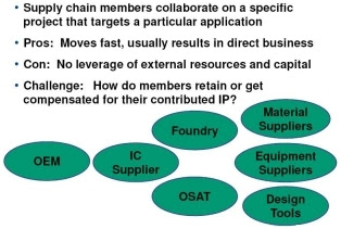
What's not quite there yet, though, according to Yu and other presenters at The ConFab, is the 3D supply chain. "3D really ties a lot of other players together and it has this really complicated cobweb type of relationship," he said. "It is, in a sense, quite disruptive to the supply chain. That's certainly one of the major challenges for a fabless company like Qualcomm. We've been spending a lot of time and resources to work with the supply chain for the last four years on this."
Qualcomm has a clear vision of what the product looks like, and that the architecture has already been optimized, Yu explained. The next step is to implement that in the manufacturing process -- and therein lies the rub. "I think there are some integration challenges out there that we haven't quite fully resolved," he said. "We need some sort of standards and conventions between the supply chain hand-offs." One example is the quality of a stack of known good die (KGD). "If we have a stack of memory, what is meant by a known good stack of memory? Who's going to be responsible for the test, and what's the quality of it?" All these discussions need to happen between the supply chain partners, with "huge implications" for their balance sheets, he noted.
Other business model questions: Who ultimately owns the dies? Who owns the inventory? And does the "pass-through" business model work? How is it going to be funded? Who owns the integration process in the end, and who owns yield? There are no easy answers and that’s part of what The ConFab is all about – giving people a forum to ask those questions and get answers.
The good news is that companies such as Qualcomm appear to be committed to making it work. "We really thought about all those challenges and we've set out to work with the industry, leveraging some of the standards bodies and really pulling together different players in the supply chain to work through that," Yu said. "There's a lot of good will and intent in the industry, but I don't think there's enough leadership."
John Waite, VP, packaging development and central engineering at GLOBALFOUNDRIES, presented noted that, since packaging costs are the dominant contributor to the value chain, designers need to select the right combination of silicon and packaging technologies to achieve performance and cost goals.
What enables success in the More Moore realm? Waite listed diverse options for wafer bumping (lead-free, copper pillar, lead and high-lead solders used in bond on pad, repassivation or redistribution [RDL] designs) and package form factor (QFP/QFN, BGA and flip chip, wafer-level chipscale packages [WLCSP]), as well as vertical options that take advantage of Z space (stacked chips, system in package [SiP]). These each have tradeoffs of cost, time, and density/performance, and customers must make packaging choices with these goals in mind.
 Packaging influences the front end. SOURCE: John Waite, GLOBALFOUNDRIES.
Packaging increasingly requires attention on the frontend because of the packaging demand on the wafer. The frontend, backend, and system suppliers must collaborate in chip development. Early engagement, EDA tool flow optimization, turnkey wafer-to-package assembly, and other risk reduction strategies take a design from R&D into high-volume manufacturing.
While integrated fabless companies are ramping up leading-edge 3D IC designs, the lack of standards is holding back the 3D ecosystem. Traditional business models also don't support the boundary-breaking 3D design and process steps. Yu supports integration via standards bodies and research consortia to bring design and manufacturing standards to the 3D arena. Consider Yu's questions: Who owns the die? Who holds the inventory? How are pass-through costs funded? Who owns the integration process? Who owns the yield? Is the additional risk of TSV worth the benefits over wire-bonded stacks? Is a fabless design company or an IDM the way to go? The key question here is who acts as the "3D aggregator"? Foundry, memory company, OEM, fabless, OSAT?
Raj Pendse, VP of product and technology marketing at STATS ChipPAC and Robert Darveaux, CTO of Amkor, covered this supply chain integration from the dedicated packaging house perspective. Pendse presented "3D Packaging Evolution from an OSAT Perspective." Darveaux spoke on "Supply Chain Challenges for 3D Integration of Memory and Logic Devices using TSVs."

Material flow and infrastructure evolution. SOURCE: Dr. Raj Pendse, STATSChipPAC Inc.
Pendse sees synergies and intersections among parallel developments in the three areas of packaging technology (i.e. traditional die and package stacking on substrates, fan-in and fan-out wafer level packaging and 3D Si integration). With these new process technologies, the OSAT industry's role is transformed. Pendse channels wafer bumping, thinning, and other tasks into an in-between space for the Si foundry and OSAT to determine logical hand off points. Many of these processes can be done in both -- the question to ask is who can do it better in each scenario? Is TSV fabrication best handled in the fab, with the OSAT taking over via fill and silicon interconnect? Pendse also spoke on "bridge" technologies -- interposers, super-thin package-on-package, TSV hybridized with fan-out wafer-level packages (FOWLP) -- that play an interim role in the commercialization of 3D. Pendse shared a typical OSAT TSV roadmap through 2013 with the attendees.
Darveaux compared the relative ease of sourcing, assembly, and test of package-on-package (POP) with the challenges of TSV: difficult to test high-density area array contact pads or bumps; bare or partially assembled memory and logic die that are difficult to burn in adequately; a newer joining technology not widely available to OEMs and contract assemblers; a poorly characterized joining process yield; and, due to the immaturity of the test, burn-in, and assembly; unclear ownership of defect liability. This applies to the "2.5D" interposer strategy as well as pure 3D TSV stacks. Interconnect processes are too new and done in too small sample sizes to lead to industry agreement on the right method: die-to-die first or die-to-laminate first? Interposer in singulated format or wafer format?

Consortium collaboration model.
Supply chain collaboration model.
SOURCE: Robert Darveaux, Amkor Technology.
These problems cannot be resolved by technologies or business models alone, he said. TSV processes can be standardized and characterized, with the resource-sharing model of consortia or the faster but potentially messy supply chain collaboration on specific projects. Both offer pros and cons, and fit different needs of the industry.
Also in 2011, Raj Jammy, VP of materials and emerging technologies at SEMATECH, covered a broad swath of CMOS scaling drivers, system and device trends, and infrastructure requirements, many of which have a direct impact on packaging. System-level trends, such as smart phones, mobile computing (e.g., iPads), and cloud computing are driving requirements for low- and ultralow-power logic with multi-core/multi-modules, dense 3D nonvolatile memory RAM for SSDs, and dense DRAMs. There is also a move to SoCs, along with high levels of functional integration and faster data transfer between modules and chips.
At the system level, the implications for devices include an even greater need for leakage reduction, and wide-band intra-chip and inter-chip interconnects. At the device level, architectural transitions to 3D FinFETs, III-V FETs, 3D flash memories, RRAM, STTRAM, SoCs, and 3D TSVs, and even photonic interconnects are being evaluated. Each of these alternatives poses specific challenges -- but common to all are strong infrastructural needs to be successful. Among the transitions' challenges will be new materials and/or using non-silicon materials, new models/test methods/designs, integration challenges, as well as processes, materials, tools, and packaging.
The biggest challenges for high-volume manufacturing of through silicon vias (TSV), Jammy said, are all through the process flow. Bonding and de-bonding is one major example, with poor throughput. Materials stresses, especially on thinned dies, are another.
SoC technologies are on the verge of some significant changes, Jammy predicts. For example, an entire smartphone could be fit onto one SoC. With system in package (SiP), additional functionality will be integrated, even MEMS devices.
Packaging has a rich history in previous ConFabs going back even further. In 2010, for example, Matt Nowak, director of engineering in Qualcomm's VLSI technology group, said high-density through-silicon stacking (TSS) shows promise for very high-volume applications, but work still needs to be done to "tame" key issues in manufacturing, improve costs, and smooth out the supply-chain. He also urged standards for supply-chain handoff points, with specs and test methods to reliably manufacture TSS from multiple sources and processes, validated by experimental results (reliability, cost, yield, etc.). Target areas for initial standards include:
• Nomenclature/definitions
• TSV size, tier thickness, via fill material
• Tier-to-tier pin locations and assignments
• Key physical design rules
• Microbump and passivation materials properties and geometries
• Reliability test methods
• Metrology
• Thin wafer shipping
Also in 2010, Jim Clifford, SVP/GM of operations at Qualcomm CDMA Technologies, talked at length about the convergence of wireless connectivity and increasing performance requirements, the resulting technical (and economic) challenges brought upon supporting technologies, and the importance of "early engagement" to cost-effectively research and develop products. He, too, stuck to a common theme across many ConFabs over the years: Collaboration across the entire eco-system. Speaking to Qualcomm's bread-and-butter, Clifford highlighted the "integrated fabless model" in which fabless companies engage with foundries very early on. In the IFM model, development starts toward the end of module development; then investing in IP/design/product development (including integration/qualification), and then production. An aligned ecosystem across the entire value chain (foundry, customers, research, EDA, IP, packaging, and testing) is required to optimize product innovation and execution. Clifford highlighted the need for early engagement with research organizations for a "co-design start," a phase dubbed "early pathfinding," which starts before and extends beyond module development and into integration/product development.
Prior to that, system-level considerations of 3D ICs were presented by Tom Gregorich, VP of Qualcomm, in a session discussing the "Economic implications of 3D" at the ConFab in Las Vegas in 2008. He reminded the audience that end-users of portable electronics products -- such as cellphones and PDA -- expect reliable functionality regardless of dropping, kicking, or washing the device. Delivering ever greater functionality in essentially the same robust package is a mandate for innovative concepts such as 3D.
Subramanian Iyer, distinguished engineer and chief technologist of IBM's Systems and Technology Group, explained the economic considerations behind 3D microprocessors. He noted that the economics of any new technology need to be assessed with respect to the advantages of other competing approaches that provide the same or similar benefits. Both embedded DRAM in a system-on-chip (SoC) and stand-alone DRAM as part of a system-in-package (SiP) have been well established as 2D solutions, so any 3D approach must be compared to these proven techniques. Iyer made his case by examining the relatively straightforward but very important challenge of balancing memory with 64 processor cores in a system.
Beyond today's stacked chips in a package may come higher performance 3D stacked ICs using through-silicon vias (TSV) to interconnect layers, according to Sitaram Arkalgud, who spoke on the economic implications of 3D.
In short, during the 8 years of The ConFab’s history, packaging topics have always been at the forefront, and will continue to be this year and in the future.
This year, for The ConFab 2012, an entire session is devoted to Advanced Packaging and Progress in 3D Integration. The session chair, Abe Yee, is Director of Advanced Technology and Package Development, Nvidia Corp. The speakers will be:
• David McCann, Senior Director for Packaging R+D, GLOBALFOUNDRIES
• Sandeep Bharathi, Vice President of Engineering, Xilinx
• Ron Huemoeller, Senior Vice President, 3DAmkor
• Bill Chen, ASE Fellow and Sr. Technical Adviser, ASE
The focus of the session will be, in part, on 3D integration which continues to offer the promise of packing ever-higher amounts of functionality into a smaller area. We’ll also be focusing on the significant progress that continues to be made in traditional packaging (such as package-on-package and wafer level packaging).
The abstracts are still coming in, but Ron Huemoeller, for example, plans to discuss some of the challenges and opportunities for high density 3DIC Through Silicon Via (TSV) product technologies in the semiconductor industry. He says that TSV product technology offers significant opportunity in the advanced product sector of the semiconductor industry as compared to traditional System on Chip (SOC) methods for packaging die. The first part of this presentation will focus on the opportunities provided by TSV product technology in the following key areas: performance and power improvement, form factor reduction and in cost reduction at the system level. The second part of this presentation will focus on the challenges remaining in bringing this new product technology to high volume production as well as anticipated product launch dates. Particular focus will be given to the issues surrounding supply chain constraint as well as the issues associated with current state of the art approaches to completing the die stacking of these complex package structures.
A strong focus on packaging was also in evidence in 2011, with a session featuring John Waite (GLOBALFOUNDRIES), Raj Pendse (STATS ChipPAC), Robert Darveaux (Amkor), and Nick Yu (Qualcomm).
• John Waite presented “Supply Chain Reaction: A Collaborative Approach to Packaging Innovation”
• Raj Pendse presented “3D Packaging Evolution from an Outsourced Semiconductor Assembly and Test (OSAT) Perspective”
• Nice Yu presented “3D Through Si Stacking Technology,” and
• Robert Darveaux presented “Supply Chain Challenges for 3D Integration of Memory and Logic Devices using TSVs.”
A recurring theme among the presentations was that 3D integration shows tremendous promise, particularly with many fabless companies, yet many barriers remain. "We firmly believe 3D will provide a better form factor and better system level performance," said Nick Yu, VP of technology development at Qualcomm. He believes that smart phones and the demand they create for wide I/O memory stacked on logic could be the key enabler for through-silicon via (TSV) technology. "We really think it can bring the best of all worlds into your mobile handset," he said. "We think the smart phone space is really the right application for 3D TSV stacking." Growth in this market drives a lot of volume, which will drive down the cost and drive adoption, thus justifying the industry's investment.

At the time, Yu said Qualcomm is pushing for implementation by 2013, and that over the last four years they have already completed a lot of engineering work with the supply chain and demonstrated the concept. It's a little bit of a "chicken-and-egg" situation, he noted, because a driver product is needed to acquire process learning and drive the product ramp, but there are "no real show-stopper or intrinsic technical issues," he said.

Supply chain needs a 3D ecosystem, as 3D is disruptive to how we do things today. SOURCE: Nick Yu, Qualcomm.
Wide I/O memory on logic provides significantly more bandwidth. The memory industry's view is that as smart phones blur the lines between tablets and hand laptops, demand for memory bandwidth will be nearly insatiable. To enable that, standards are needed and JEDEC is going to finish the wide memory standardization by the end of 2011. Memory vendors will have parts sampling in 2012, all targeting end-product going to market by 2013, according to Yu (again, speaking in 2011).
What's not quite there yet, though, according to Yu and other presenters at The ConFab, is the 3D supply chain. "3D really ties a lot of other players together and it has this really complicated cobweb type of relationship," he said. "It is, in a sense, quite disruptive to the supply chain. That's certainly one of the major challenges for a fabless company like Qualcomm. We've been spending a lot of time and resources to work with the supply chain for the last four years on this."
Other business model questions: Who ultimately owns the dies? Who owns the inventory? And does the "pass-through" business model work? How is it going to be funded? Who owns the integration process in the end, and who owns yield? There are no easy answers and that’s part of what The ConFab is all about – giving people a forum to ask those questions and get answers.
The good news is that companies such as Qualcomm appear to be committed to making it work. "We really thought about all those challenges and we've set out to work with the industry, leveraging some of the standards bodies and really pulling together different players in the supply chain to work through that," Yu said. "There's a lot of good will and intent in the industry, but I don't think there's enough leadership."
John Waite, VP, packaging development and central engineering at GLOBALFOUNDRIES, presented noted that, since packaging costs are the dominant contributor to the value chain, designers need to select the right combination of silicon and packaging technologies to achieve performance and cost goals.
What enables success in the More Moore realm? Waite listed diverse options for wafer bumping (lead-free, copper pillar, lead and high-lead solders used in bond on pad, repassivation or redistribution [RDL] designs) and package form factor (QFP/QFN, BGA and flip chip, wafer-level chipscale packages [WLCSP]), as well as vertical options that take advantage of Z space (stacked chips, system in package [SiP]). These each have tradeoffs of cost, time, and density/performance, and customers must make packaging choices with these goals in mind.

Packaging increasingly requires attention on the frontend because of the packaging demand on the wafer. The frontend, backend, and system suppliers must collaborate in chip development. Early engagement, EDA tool flow optimization, turnkey wafer-to-package assembly, and other risk reduction strategies take a design from R&D into high-volume manufacturing.
While integrated fabless companies are ramping up leading-edge 3D IC designs, the lack of standards is holding back the 3D ecosystem. Traditional business models also don't support the boundary-breaking 3D design and process steps. Yu supports integration via standards bodies and research consortia to bring design and manufacturing standards to the 3D arena. Consider Yu's questions: Who owns the die? Who holds the inventory? How are pass-through costs funded? Who owns the integration process? Who owns the yield? Is the additional risk of TSV worth the benefits over wire-bonded stacks? Is a fabless design company or an IDM the way to go? The key question here is who acts as the "3D aggregator"? Foundry, memory company, OEM, fabless, OSAT?
Raj Pendse, VP of product and technology marketing at STATS ChipPAC and Robert Darveaux, CTO of Amkor, covered this supply chain integration from the dedicated packaging house perspective. Pendse presented "3D Packaging Evolution from an OSAT Perspective." Darveaux spoke on "Supply Chain Challenges for 3D Integration of Memory and Logic Devices using TSVs."

Material flow and infrastructure evolution. SOURCE: Dr. Raj Pendse, STATSChipPAC Inc.
Pendse sees synergies and intersections among parallel developments in the three areas of packaging technology (i.e. traditional die and package stacking on substrates, fan-in and fan-out wafer level packaging and 3D Si integration). With these new process technologies, the OSAT industry's role is transformed. Pendse channels wafer bumping, thinning, and other tasks into an in-between space for the Si foundry and OSAT to determine logical hand off points. Many of these processes can be done in both -- the question to ask is who can do it better in each scenario? Is TSV fabrication best handled in the fab, with the OSAT taking over via fill and silicon interconnect? Pendse also spoke on "bridge" technologies -- interposers, super-thin package-on-package, TSV hybridized with fan-out wafer-level packages (FOWLP) -- that play an interim role in the commercialization of 3D. Pendse shared a typical OSAT TSV roadmap through 2013 with the attendees.
Darveaux compared the relative ease of sourcing, assembly, and test of package-on-package (POP) with the challenges of TSV: difficult to test high-density area array contact pads or bumps; bare or partially assembled memory and logic die that are difficult to burn in adequately; a newer joining technology not widely available to OEMs and contract assemblers; a poorly characterized joining process yield; and, due to the immaturity of the test, burn-in, and assembly; unclear ownership of defect liability. This applies to the "2.5D" interposer strategy as well as pure 3D TSV stacks. Interconnect processes are too new and done in too small sample sizes to lead to industry agreement on the right method: die-to-die first or die-to-laminate first? Interposer in singulated format or wafer format?

Consortium collaboration model.

Supply chain collaboration model.
SOURCE: Robert Darveaux, Amkor Technology.
These problems cannot be resolved by technologies or business models alone, he said. TSV processes can be standardized and characterized, with the resource-sharing model of consortia or the faster but potentially messy supply chain collaboration on specific projects. Both offer pros and cons, and fit different needs of the industry.
Also in 2011, Raj Jammy, VP of materials and emerging technologies at SEMATECH, covered a broad swath of CMOS scaling drivers, system and device trends, and infrastructure requirements, many of which have a direct impact on packaging. System-level trends, such as smart phones, mobile computing (e.g., iPads), and cloud computing are driving requirements for low- and ultralow-power logic with multi-core/multi-modules, dense 3D nonvolatile memory RAM for SSDs, and dense DRAMs. There is also a move to SoCs, along with high levels of functional integration and faster data transfer between modules and chips.
At the system level, the implications for devices include an even greater need for leakage reduction, and wide-band intra-chip and inter-chip interconnects. At the device level, architectural transitions to 3D FinFETs, III-V FETs, 3D flash memories, RRAM, STTRAM, SoCs, and 3D TSVs, and even photonic interconnects are being evaluated. Each of these alternatives poses specific challenges -- but common to all are strong infrastructural needs to be successful. Among the transitions' challenges will be new materials and/or using non-silicon materials, new models/test methods/designs, integration challenges, as well as processes, materials, tools, and packaging.
The biggest challenges for high-volume manufacturing of through silicon vias (TSV), Jammy said, are all through the process flow. Bonding and de-bonding is one major example, with poor throughput. Materials stresses, especially on thinned dies, are another.
SoC technologies are on the verge of some significant changes, Jammy predicts. For example, an entire smartphone could be fit onto one SoC. With system in package (SiP), additional functionality will be integrated, even MEMS devices.
Packaging has a rich history in previous ConFabs going back even further. In 2010, for example, Matt Nowak, director of engineering in Qualcomm's VLSI technology group, said high-density through-silicon stacking (TSS) shows promise for very high-volume applications, but work still needs to be done to "tame" key issues in manufacturing, improve costs, and smooth out the supply-chain. He also urged standards for supply-chain handoff points, with specs and test methods to reliably manufacture TSS from multiple sources and processes, validated by experimental results (reliability, cost, yield, etc.). Target areas for initial standards include:
• Nomenclature/definitions
• TSV size, tier thickness, via fill material
• Tier-to-tier pin locations and assignments
• Key physical design rules
• Microbump and passivation materials properties and geometries
• Reliability test methods
• Metrology
• Thin wafer shipping
Also in 2010, Jim Clifford, SVP/GM of operations at Qualcomm CDMA Technologies, talked at length about the convergence of wireless connectivity and increasing performance requirements, the resulting technical (and economic) challenges brought upon supporting technologies, and the importance of "early engagement" to cost-effectively research and develop products. He, too, stuck to a common theme across many ConFabs over the years: Collaboration across the entire eco-system. Speaking to Qualcomm's bread-and-butter, Clifford highlighted the "integrated fabless model" in which fabless companies engage with foundries very early on. In the IFM model, development starts toward the end of module development; then investing in IP/design/product development (including integration/qualification), and then production. An aligned ecosystem across the entire value chain (foundry, customers, research, EDA, IP, packaging, and testing) is required to optimize product innovation and execution. Clifford highlighted the need for early engagement with research organizations for a "co-design start," a phase dubbed "early pathfinding," which starts before and extends beyond module development and into integration/product development.
Prior to that, system-level considerations of 3D ICs were presented by Tom Gregorich, VP of Qualcomm, in a session discussing the "Economic implications of 3D" at the ConFab in Las Vegas in 2008. He reminded the audience that end-users of portable electronics products -- such as cellphones and PDA -- expect reliable functionality regardless of dropping, kicking, or washing the device. Delivering ever greater functionality in essentially the same robust package is a mandate for innovative concepts such as 3D.
Subramanian Iyer, distinguished engineer and chief technologist of IBM's Systems and Technology Group, explained the economic considerations behind 3D microprocessors. He noted that the economics of any new technology need to be assessed with respect to the advantages of other competing approaches that provide the same or similar benefits. Both embedded DRAM in a system-on-chip (SoC) and stand-alone DRAM as part of a system-in-package (SiP) have been well established as 2D solutions, so any 3D approach must be compared to these proven techniques. Iyer made his case by examining the relatively straightforward but very important challenge of balancing memory with 64 processor cores in a system.
Beyond today's stacked chips in a package may come higher performance 3D stacked ICs using through-silicon vias (TSV) to interconnect layers, according to Sitaram Arkalgud, who spoke on the economic implications of 3D.
In short, during the 8 years of The ConFab’s history, packaging topics have always been at the forefront, and will continue to be this year and in the future.
Subscribe to:
Posts (Atom)